
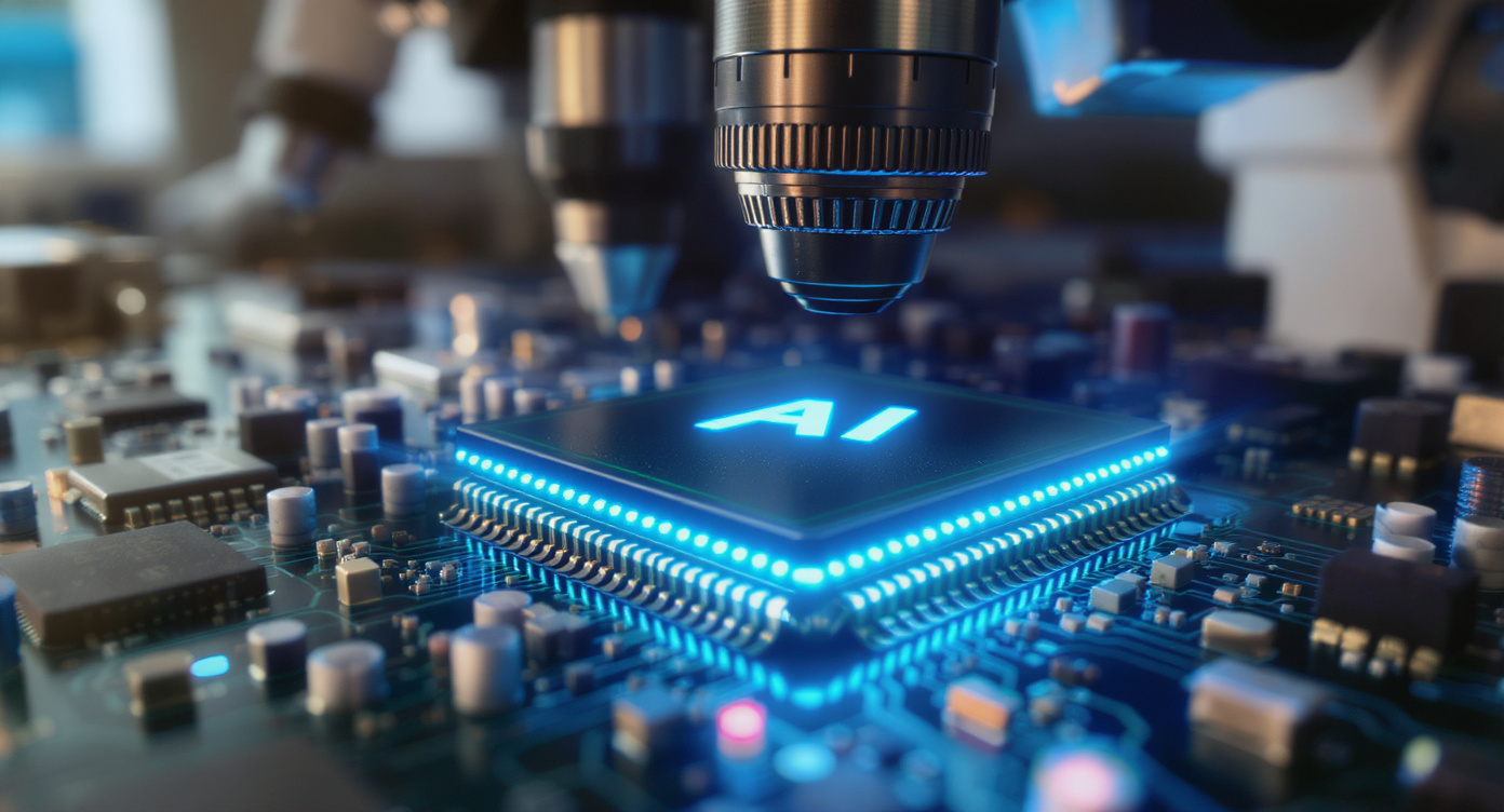
The semiconductor industry has just witnessed a monumental leap forward that could reshape the entire landscape of artificial intelligence computing. Taiwan Semiconductor Manufacturing Company (TSMC), the world’s leading contract chip manufacturer, has successfully developed 2-nanometer (2nm) process technology specifically optimized for AI applications. This breakthrough represents more than just a numerical advancement—it’s a paradigm shift that promises to unlock unprecedented capabilities in machine learning, edge computing, and intelligent systems across every industry.
TSMC’s achievement in reaching the 2nm node represents the culmination of years of intensive research and development, pushing the boundaries of what’s physically possible in semiconductor manufacturing. At this scale, we’re dealing with transistors that are just a few atoms wide, requiring revolutionary approaches to lithography, materials science, and manufacturing precision. The implications extend far beyond faster processors; we’re looking at a fundamental transformation in how AI systems consume power, process information, and integrate into our daily lives.
The Technical Marvel Behind 2nm AI Chips
The transition from 3nm to 2nm technology might seem like a simple mathematical progression, but the engineering challenges involved are exponentially complex. At the 2nm node, TSMC has managed to pack approximately 33 billion transistors into a single square centimeter—a density that seemed impossible just a decade ago. This incredible miniaturization is achieved through advanced extreme ultraviolet (EUV) lithography techniques and novel materials that maintain electrical properties at atomic scales.
What makes these 2nm chips particularly revolutionary for AI applications is their specialized architecture. Unlike traditional processors designed for general computing tasks, these chips incorporate dedicated neural processing units (NPUs) that can handle matrix multiplications and tensor operations with remarkable efficiency. The 2nm process allows for more complex on-chip memory hierarchies, reducing the need for external memory access and dramatically improving performance per watt.
The power efficiency gains are perhaps the most significant advantage. TSMC’s 2nm AI chips consume up to 30% less power than their 3nm predecessors while delivering 15-20% better performance. This improvement isn’t just about better battery life in mobile devices—it’s about making AI processing economically viable for applications that were previously too power-hungry to implement practically.
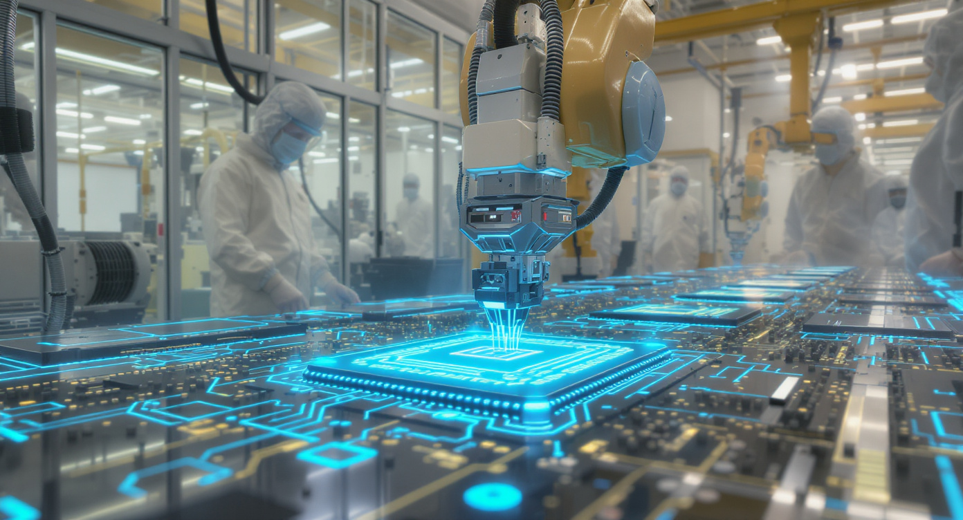
Manufacturing at this scale requires unprecedented precision. TSMC’s fabrication facilities, known as “fabs,” must maintain cleanliness levels that exceed those of operating rooms by several orders of magnitude. The company has invested over $40 billion in developing the infrastructure necessary to produce 2nm chips at scale, including new fabrication equipment that costs hundreds of millions of dollars per unit.
Game-Changing Applications Across Industries
The arrival of 2nm AI chips is set to catalyze transformative changes across multiple sectors, enabling applications that were previously constrained by processing power and energy consumption limitations. In the automotive industry, these chips will accelerate the deployment of fully autonomous vehicles by providing the computational horsepower needed for real-time processing of sensor data from cameras, lidar, and radar systems. The improved power efficiency means longer operational ranges for electric autonomous vehicles, addressing one of the key barriers to widespread adoption.
Healthcare applications represent another frontier where 2nm AI chips will drive significant innovation. Portable diagnostic devices powered by these chips can perform complex medical imaging analysis in remote locations, bringing advanced healthcare capabilities to underserved regions. Real-time genomic analysis, personalized treatment recommendations, and continuous health monitoring through wearable devices become practical realities when powered by energy-efficient, high-performance AI processors.
The smartphone and mobile device ecosystem will experience a renaissance with 2nm AI chips. Enhanced computational photography, real-time language translation, advanced augmented reality applications, and sophisticated personal assistants will operate seamlessly on mobile devices without draining battery life. The improved processing capabilities enable on-device AI processing for privacy-sensitive applications, reducing dependence on cloud-based services and improving response times.
Data centers and cloud computing infrastructure will also benefit dramatically from 2nm AI chips. The improved performance-per-watt ratio means that cloud providers can deliver more AI processing capabilities while reducing their energy consumption and cooling requirements. This efficiency gain translates directly into cost savings that can be passed on to customers, making AI services more accessible to smaller businesses and individual developers.
Edge computing applications, from smart city infrastructure to industrial IoT devices, become more sophisticated and capable with 2nm AI chips. These processors can handle complex machine learning tasks locally, reducing latency and bandwidth requirements while improving system reliability and data privacy.
Market Impact and Industry Transformation
TSMC’s 2nm breakthrough is reshaping competitive dynamics across the technology sector, creating new opportunities while disrupting established market positions. Companies that can effectively leverage these advanced chips will gain significant competitive advantages, while those that fail to adapt risk being left behind in an increasingly AI-driven marketplace.
The semiconductor industry itself is experiencing a fundamental shift in investment priorities and strategic focus. Traditional chip designers are pivoting toward AI-optimized architectures, while new startups are emerging with innovative approaches to AI chip design specifically tailored for 2nm processes. This technological advancement is also accelerating consolidation in the industry, as smaller players struggle to keep pace with the massive capital investments required for cutting-edge development.
From an economic perspective, the availability of 2nm AI chips is catalyzing the growth of entirely new market segments. AI-as-a-Service platforms become more cost-effective and powerful, enabling smaller companies to access sophisticated machine learning capabilities without massive infrastructure investments. The democratization of AI processing power is fostering innovation across industries that previously couldn’t justify the costs associated with advanced AI implementations.
Supply chain implications are equally significant. TSMC’s leadership in 2nm technology strengthens Taiwan’s position as a critical hub in the global semiconductor ecosystem, while creating strategic dependencies that governments and corporations must carefully manage. The complexity and cost of 2nm fabrication mean that only a few companies worldwide can realistically compete at this technological frontier, concentrating advanced chip production in the hands of a select few manufacturers.
The talent market is responding rapidly to these developments, with unprecedented demand for engineers specializing in AI chip design, advanced semiconductor processes, and related technologies. Universities and research institutions are adapting their curricula to address the skills gap, while established professionals are investing heavily in retraining to remain relevant in this rapidly evolving landscape.
Overcoming Challenges and Future Implications
Despite the revolutionary potential of 2nm AI chips, several significant challenges must be addressed to realize their full impact. Manufacturing complexity and yield rates represent ongoing concerns, as the extreme precision required for 2nm processes makes production susceptible to minute variations that can affect chip performance and reliability. TSMC continues to refine its manufacturing processes to improve yields and reduce costs, but the inherent challenges of working at atomic scales mean that progress requires sustained investment and innovation.
Thermal management becomes increasingly critical at the 2nm node, as the high density of transistors creates localized heat generation that can affect performance and longevity. Advanced packaging technologies and innovative cooling solutions are essential to fully exploit the capabilities of these chips while maintaining reliability standards required for commercial applications.
The software ecosystem must also evolve to take full advantage of 2nm AI chips’ capabilities. Existing machine learning frameworks and development tools need optimization for the unique architectural features of these processors. This software evolution requires collaboration between chip manufacturers, software developers, and the broader AI research community to ensure that theoretical hardware capabilities translate into practical performance improvements.
Looking ahead, TSMC’s 2nm breakthrough is just the beginning of a new era in AI computing. The company is already researching next-generation processes, including 1.4nm and beyond, while exploring alternative approaches such as 3D chip architectures and novel materials that could extend Moore’s Law even further. The integration of quantum computing elements with traditional silicon processes represents another frontier that could emerge from current 2nm research.
The geopolitical implications of advanced semiconductor technology continue to evolve, with governments worldwide recognizing the strategic importance of AI chip capabilities. Investment in domestic semiconductor manufacturing capabilities is increasing globally, though the technical and financial barriers to competing with established leaders like TSMC remain substantial.
TSMC’s achievement in bringing 2nm AI chips to market represents a watershed moment that will influence technological development for years to come. The combination of unprecedented processing power, improved energy efficiency, and specialized AI optimization creates opportunities for innovation across every sector of the economy. While challenges remain in manufacturing, thermal management, and software optimization, the potential benefits far outweigh the obstacles.
As we stand at the threshold of this new era in AI computing, the question isn’t whether 2nm chips will transform our world, but how quickly and comprehensively that transformation will occur. The companies, industries, and nations that recognize and act upon this shift will define the next chapter of technological progress.
What industry or application do you think will be most dramatically transformed by the availability of 2nm AI chips, and how are you preparing your organization to leverage these revolutionary capabilities?
Comments