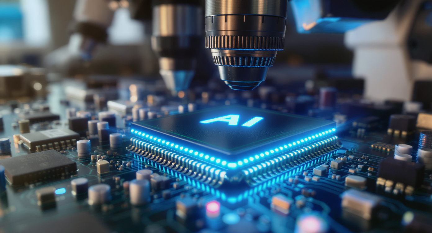
The semiconductor industry has just witnessed a monumental leap forward as Taiwan Semiconductor Manufacturing Company (TSMC) achieves the highly anticipated 2-nanometer (2nm) chip manufacturing milestone. This breakthrough represents more than just a numerical advancement—it’s a paradigm shift that promises to revolutionize artificial intelligence computing, reshape competitive landscapes, and unlock unprecedented possibilities in tech innovation.
As we stand at the precipice of this technological revolution, the implications extend far beyond the confines of silicon wafers and fabrication facilities. TSMC’s 2nm achievement signals the dawn of a new era where AI chips will deliver exponentially greater performance while consuming significantly less power, fundamentally changing how we interact with technology in our daily lives.
What Makes 2nm Technology Truly Game-Changing
The transition from 3nm to 2nm technology represents a quantum leap in semiconductor engineering that goes beyond simple size reduction. At the 2nm node, transistors are now approaching atomic-scale dimensions, with each transistor measuring approximately 10-12 atoms wide. This incredible miniaturization enables chip designers to pack an astounding number of transistors into the same space, dramatically increasing computational density.
Performance and Efficiency Gains
TSMC’s 2nm process technology delivers remarkable improvements across all critical metrics. Early projections suggest that 2nm chips will offer:
- 15-20% performance improvement over 3nm predecessors at the same power consumption
- 25-30% power reduction while maintaining equivalent performance levels
- Logic density improvements of up to 1.1x compared to 3nm technology
These enhancements translate into tangible benefits for AI applications, where computational intensity and power efficiency are paramount concerns. Machine learning algorithms, neural network processing, and real-time AI inference will experience dramatic acceleration, enabling more sophisticated AI capabilities in everything from smartphones to autonomous vehicles.
Manufacturing Innovation at the Atomic Level
The technical challenges overcome in achieving 2nm production are staggering. TSMC has pioneered advanced techniques including:
- Gate-All-Around (GAA) nanosheet transistors that provide superior electrostatic control
- Extreme Ultraviolet (EUV) lithography with multiple patterning layers
- Advanced materials engineering to manage quantum effects at atomic scales
- Precision metrology systems capable of measuring variations at the sub-nanometer level
These innovations represent years of research and development, with TSMC investing over $40 billion in advanced manufacturing capabilities and R&D initiatives.
Impact on AI Computing and Performance
The advent of 2nm AI chips creates a multiplier effect across the entire artificial intelligence ecosystem. This technological advancement addresses several critical bottlenecks that have constrained AI development and deployment.
Edge AI Revolution
One of the most significant impacts will be felt in edge AI applications. The combination of increased performance and reduced power consumption makes it feasible to deploy sophisticated AI models directly on mobile devices, IoT sensors, and embedded systems. This shift eliminates the latency and privacy concerns associated with cloud-based AI processing while enabling real-time decision-making at the point of data collection.
Consider the implications for autonomous vehicles: 2nm AI chips can process vast amounts of sensor data instantaneously, enabling faster reaction times and more accurate environmental understanding. Similarly, smartphones equipped with 2nm processors will run complex AI applications—from advanced photography algorithms to real-time language translation—without draining battery life.
Data Center Efficiency Transformation
In data center environments, 2nm AI chips promise to reshape the economics of large-scale AI training and inference. The improved power efficiency directly translates to reduced operational costs and lower carbon footprints, addressing growing concerns about the environmental impact of AI computing.
Major cloud providers and AI companies can expect:
- Reduced cooling requirements due to lower heat generation
- Higher compute density in existing rack space
- Improved total cost of ownership over the chip lifecycle
- Enhanced AI model capabilities within existing power budgets
Breakthrough AI Applications
The performance headroom created by 2nm technology will enable entirely new categories of AI applications that were previously computationally prohibitive. Real-time video analysis, advanced natural language processing, and complex scientific simulations will become more accessible and practical for widespread deployment.
Industry Implications and Competitive Landscape
TSMC’s 2nm breakthrough fundamentally alters the competitive dynamics within the semiconductor industry and creates ripple effects throughout the entire technology sector.
Market Leadership Consolidation
This achievement further solidifies TSMC’s position as the world’s premier contract chip manufacturer, with the company now commanding an estimated 60% market share in advanced logic semiconductors. The technical complexity and enormous capital requirements for 2nm production create significant barriers to entry, effectively limiting the number of companies capable of competing at the cutting edge.
Supply Chain Concentration Risks
While TSMC’s leadership benefits customers through technological advancement, it also creates concerning concentration risks for the global technology supply chain. Major technology companies including Apple, NVIDIA, AMD, and Qualcomm rely heavily on TSMC for their most advanced chips, creating potential vulnerabilities during geopolitical tensions or natural disasters.
Geopolitical Technology Competition
The 2nm milestone intensifies the global race for semiconductor supremacy, particularly between the United States, Taiwan, and China. Governments worldwide are recognizing advanced chip manufacturing as a critical national security capability, leading to unprecedented investments in domestic semiconductor production capabilities.
The U.S. CHIPS Act, European Chips Act, and China’s massive semiconductor investment programs all reflect this strategic imperative. However, TSMC’s technical leadership and manufacturing expertise create a significant competitive moat that will be challenging for competitors to overcome in the near term.
Customer Strategy Evolution
Technology companies are increasingly designing their product roadmaps around TSMC’s manufacturing capabilities, creating a symbiotic relationship between chip designers and the foundry. This dynamic influences everything from AI accelerator architectures to smartphone feature development, with companies planning products 3-5 years in advance based on expected manufacturing node availability.
Future Outlook and What This Means for Tech Innovation
The successful commercialization of 2nm technology sets the stage for continued innovation in AI computing and broader technology applications, even as the industry approaches fundamental physical limits.
Timeline for Mass Production
TSMC expects to begin risk production of 2nm chips in 2024, with high-volume manufacturing targeted for 2025. The initial focus will be on premium applications where customers can justify the higher production costs, including flagship smartphones, high-performance AI accelerators, and advanced automotive chips.
As manufacturing volumes increase and yields improve throughout 2025-2026, 2nm technology will gradually expand to broader market segments, eventually reaching mainstream applications by the late 2020s.
Beyond 2nm: The Path Forward
While 2nm represents a significant milestone, TSMC is already researching even more advanced nodes, including 1.4nm and 1nm technologies. However, the industry is rapidly approaching fundamental physical limits where traditional scaling approaches may no longer be viable.
Future advancement will likely require:
- Novel materials beyond traditional silicon
- Three-dimensional chip architectures for continued density improvements
- Quantum computing integration for specific computational tasks
- Neuromorphic computing designs that mimic brain-like processing patterns
Transformative Application Potential
The capabilities unlocked by 2nm AI chips will enable transformative applications across multiple industries:
- Healthcare: Real-time medical imaging analysis and personalized treatment optimization
- Transportation: Fully autonomous vehicle navigation and traffic optimization systems
- Energy: Smart grid management and renewable energy optimization
- Manufacturing: Predictive maintenance and automated quality control systems
- Communication: Advanced real-time language translation and augmented reality experiences
The convergence of 2nm chip capabilities with advances in AI algorithms and software architectures promises to accelerate innovation across virtually every technology-dependent industry.
TSMC’s achievement of 2nm technology represents more than an incremental improvement—it’s a catalyst that will reshape the AI landscape and enable the next generation of intelligent applications. As these advanced chips move from laboratory prototypes to mass production, we’ll witness unprecedented capabilities in AI performance, efficiency, and accessibility.
The implications extend beyond technical specifications to fundamental questions about technological sovereignty, competitive advantage, and the future of human-machine interaction. Organizations across industries must prepare for the transformative potential of 2nm AI chips while navigating the complex geopolitical and economic realities of advanced semiconductor manufacturing.
How do you think 2nm AI chips will transform your industry, and what steps is your organization taking to prepare for this technological leap?

Comments